![]()
![]()
![]()
![]()
The Optics Laboratory
Group of
Hans Hallen, North Carolina State University Physics Department![]()
Imaging the Recombination Lifetime.
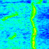
Three images show the same 20 micron square region of an oxygen terminated silicon surface with different contrast methods. (left) A topographic image of the region shown with a 240 nm vertical gray scale range and with white higher. (center) The infrared transmission (0.44 nW range with a ~80 nW dc background subtraction) shows regions of contrast, red more intense, near some of the multiple step defects and on some terrace areas. (right) The time-resolved image of IR amplitude change while the visible light is switched reveals regions near part of the multiple step defects which have a faster recombination rate (green). The range is 0.038 nW.


![]()
The center image acts as a control to insure that the effect isn't simply due to an artifact in the IR reflection. We see that the image is not correlated to the recombination image on the right. It shows some variation near some of the multiple-step edges seen in the stepped topography on the left, and some variation on the terraces. The variation on the terraces is likely due to adsorbates with a higher index of refraction, which can duct more of the near-field light into the sample.
To understand the image on the right, we must get a qualitative understanding of the recombination rate vs. the contrast. The general idea is shown here:
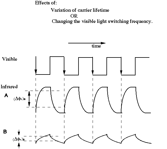
The infrared (number of carriers) signal follows the inverse of the visible signal as best it can given its time constant. For fast recombination (A), it can follow approximately, so a large IR variation is obtained. For a recombination rate slow compared to the visible light switching frequency, (B), the infrared oscillations never saturate, and the net amplitude is much smaller. Perhaps this has some zero-offset, but it is unimportant since the lock-in amplifier measures only the oscillation amplitude. We then understand the image as follows: high level (green, yellow) are fast recombination rates, low level (blue) are slow recombination rates.
The fast recombination rate near a topographic step makes sense. This is a likely location for defects in the surface passivation. Such defects are known to reduce the recombination lifetime due to the creation of mid-gap states.
Next we turn to the effects when imaging at different visible light switching frequencies. First, we plot the lock-in output as a function of frequency.

Note that it behaves as expected given the discussion above. The frequency at which the response falls is related to the lifetime and will be discussed in ‘quantification.’ Now, we image where the low frequency behavior is still strong and at two frequencies above where it has significantly fallen.
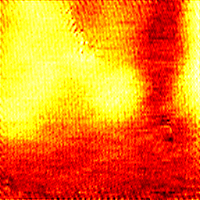
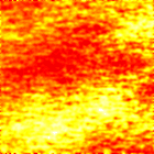
The effects of varying the visible light switching frequency in 7.5
mm square images of nearly the same area on the 'circle' sample (white high, red, black low) are shown. (left) An image of the IR signal change as the visible light is switched on and off at 100 Hz with 0.27 nW range. (center) As (left), but at a frequency of 2 kHz, 0.03 nW range. (right) At 20 kHz modulation, 0.03 nW range.Note that the two at higher frequencies are similar, but different than that where the carrier lifetime effects are noticeable. The image on the left is a map of recombination lifetime as above. Those on the right are maps of a faster process that operates in series with the carrier recombination. We know this because the plot vs. frequency does not go to zero, but remains finite throughout the measurement range. It will eventually drop off, at frequencies above the response rate of the faster process: carrier diffusion. On the length scales considered here, diffusion is very fast. Carriers in silicon can diffuse from under the probe on average in nanoseconds. The differences in the two higher frequency images are primarily caused by remnants of the recombination process still visible in the image at the lower of the two frequencies.
![]()
![]()
Last updated on October 5, 2000