![]()
![]()
![]()
![]()
The Optics Laboratory
Group of
Hans Hallen, North Carolina State University Physics Department![]()
SOI Samples, Carrier Recombination and Diffusion Compete
Silicon on Insulator samples are produced so that electronics produced on the crystalline silicon will have less capacitance to the wafer bulk. This reduces current drive requirements for wiring or, equivalently, allows faster performance (RC times are faster).
The thin silicon layer changes the diffusion. If it is very thin, the carriers can diffuse away only in two dimensions rather than three. This qualitatively changes the diffusion profile and increases the trapped carrier density. In practice, either the layers are usually thick enough that this is not important, or the layers are uniform enough in thickness that the effect is the same at all points in an NSOM image. But some (relatively rare) parts of the SOI wafers we studied behave very differently than the recombination at low frequencies/diffusion at higher frequencies picture.
First, the typical regions are presented. The samples used here were silicon-on-insulator (SOI) produced by oxygen implantation and annealing. The buried oxide is ~ 400 nm thick, under ~ 120 - 130 nm of silicon. No special termination of the outer silicon surface was used. The carrier effective lifetime of this sample, = 1 µs, was measured at room temperature using a laser/microwave method (Lifetech-88, Semitex Co., Ltd):
(a) (b) (c)

(d)
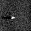
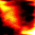
The ten micron square scanned region is shown in gray scale. (a) shows the topography range with range 50 nm, (b) shows the IR intensity with range 1.5 nW after a 21 nW background subtraction, (c) shows the time-resolved image using the phase of the modulated signal with range 24 degrees, and (d) shows the frequency dependence of the IR magnitude modulation with visible light modulation frequency.
As we have seen before, no strong correlation between the infrared transmission and the time resolved image is observed. The arrow in (d) points to the plateau just before the drop due to the local recombination time. The drop at lower frequencies is related to the time constant of the probe heating and cooling, and is described in detail in our papers. The images are taken at higher frequencies, so are not effected by the probe time response.
Another region shows the unusual response:
(a)

(b) (c)
(d) (e).
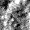
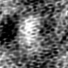
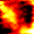
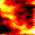
NSOM images of an SOI sample. All images correspond to the same region of 7.5 µm x 7.5 µm. (a) Sample topography derived from a shear-force feedback (the gray scale range is 15 nm - black higher). (b) The infrared transmitted intensity as a function of position with 0.3 nW range (white higher) and a 5 nW background subtracted. (c-e) The time-resolved images taken at the following frequencies, RMS range: (c) 170 Hz, 6.2 pW, (d) 750 Hz, 4.5 pW, and (e) 8.5 kHz, 2.5 pW.
A strong influence of the transmitted infrared signal is observed in the time-resolved images, although the resolution varies. The topographic image reveals that the thickness of either the top Si or the buried oxide or both vary across the analyzed region. A possible explanation for the data is that thickness variations in the silicon trap carriers in local regions, surrounded by thinner than average silicon on one or more sides. More carriers means that both the DC and AC responses are larger. On SOI or similar samples, this technique may prove useful as a uniformity tester with nanoscale resolution.
![]()
![]()
Last updated on October 5, 2000